
Semiconductor failure analysis employs techniques from visual inspection to advanced spectroscopy to ensure device reliability and adherence to Moore's law.
By Nidhi DhullMar 8 2024Reviewed by Megan Craig, M.Sc. Failure analysis is an essential part of a complex reliability evaluation in the semiconductor industry. In an industrial environment, failure analysis may start from a preliminary analysis through a generalized flow chart and end up with in-depth advanced techniques.1 The first step for semiconductor chips is visual inspection using an optical microscope or electrical measurements.
The detection of a failure and its rapid solution in a laboratory environment is crucial for large-scale manufacturing of miniaturized semiconductors.4 Failure analysis is important to ensure that the semiconductor industry successfully keeps up with Moore’s law, which estimates a doubling of the number of transistors in an integrated circuit about every two years.
Scanning electron microscope allows analysis of a semiconductor surface and cross-section with high resolution, revealing contamination, cracking, or thermal damage. Additionally, electrical defects in semiconductors can be identified by irradiating them with an SEM’s electron beam and detecting the current or voltage thus generated.1
Semiconductor failure analysis in terms of the thermal properties of a sample is performed using techniques like fluorescent micro-thermography, infrared thermography, and photothermal radiometry. These techniques are material-specific and give information about heat capacity, thermal conductivity, film thickness, material inhomogeneities, and delaminations.2
The atomic constitution of the impurities can be estimated using energy-dispersive X-ray spectroscopy. . It also reveals the 2D distribution of an element in comparison to the SEM image from the same area. This method is used in catastrophic failure analysis like electrode degradation or solder migration in a device.1
Case Studies and Applications Lately, AI tools are being implemented for semiconductor failure analysis. A recent study published in ACS Applied Nano Materials demonstrated the effectiveness of AI-integrated physical modeling on the electrical response of the device. It was able to reveal defects equivalent to a needle-in-a-haystack.
日本 最新ニュース, 日本 見出し
Similar News:他のニュース ソースから収集した、これに似たニュース記事を読むこともできます。
 Electrical AFM, An Indispensable Tool in the Semiconductor IndustryElectrical AFM is crucial in semiconductor manufacturing, offering nanoscale resolution for device inspection and material analysis.
続きを読む »
 alpha300 Semiconductor Edition – Raman imaging microscope for large wafer inspectionThis product profile describes the features and applications of the alpha300 Semiconductor Edition Raman microscope for chemical imaging.
続きを読む »
 Certificate Validation Failure Causes Issue in ServerA recent report reveals that a certificate validation failure has caused an issue in a server. The server runs its own certificate authority (CA) and uses it to sign certificates for all devices. The failure occurred because the system couldn't check the certificate revocation list (CRL).
続きを読む »
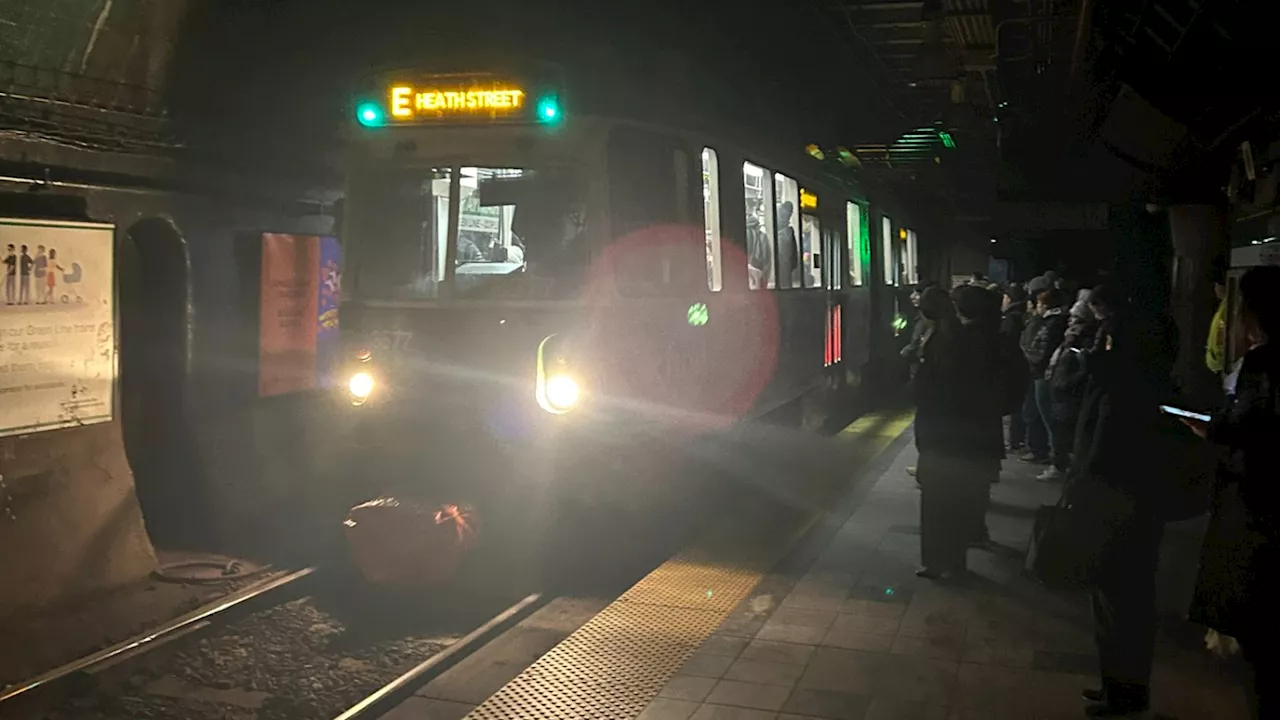 Power failure knocks out 3 T lines during commute; ‘We apologize,' GM saysA major power outage badly disrupted service on three MBTA lines during the morning commute Thursday, causing a blackout at at least one station. Riders were…
続きを読む »
 Train delays and cancellations as South East hit by signal failureA power failure causes delays and cancellations to trains in south-east England, including Gatwick.
続きを読む »
 Lincoln woman with kidney failure accused of wasting NHS resourcesLincoln and Greater Lincolnshire news
続きを読む »