
Accurate stress measurement in thin films is crucial for the performance and reliability of products in various high-tech industries.
By Susha Cheriyedath, M.Sc.Feb 16 2024Reviewed by Megan Craig, M.Sc. Discover the significance of stress measurement in thin films for industries like semiconductors and medical equipment, and explore various methods for precise quantification. Thin films form the basis of many industries today, including semiconductors, electric vehicles, smart optical coatings, sophisticated medical equipment, and protective layers on high-temperature alloys.
See our full range of equipment. The nature of the stress highly depends on the deposition technique. For instance, sputtering yields compressed films, while films from chemical vapor deposition are tensed.2 Phase transformations, such as from amorphous to polycrystalline during post-deposition thermal treatments, may add to the film stress.2 The deformations that occur to thin films can be macroscopically measured in terms of a change in curvature on their surfaces.
Methods and Techniques for Stress Measurement in Thin Films With recent technological advancements, several methods and techniques have evolved for near-to-exact stress measurements. These involve either measuring the substrate deformation produced by the stress in the film and then calculating the stress or measuring the strain in the film and then calculating the stress using Hooke’s law.
In the case of reflecting surfaces, a widely used technique involves measuring the deflection of a laser beam reflected from the sample as it is scanned across its surface. Multi-beam optical sensor is one such stress measuring tool developed by k-Space ASSOCIATES, INC that uses a laser beam to measure the thin films' curvature in situ optically during the deposition process. 1Raman spectroscopy is also widely used to measure strain in silicon substrates with high spatial resolution.
Applications of Stress Measurement in Thin Film Characterization Microstructural characteristics of thin films, such as grain size and grain morphology, thermal and electrical transport, and optical properties, can vary widely with deposition techniques. Internal residual stresses retained in thin films due to the deposition process significantly influence the microstructural properties of the films.
日本 最新ニュース, 日本 見出し
Similar News:他のニュース ソースから収集した、これに似たニュース記事を読むこともできます。
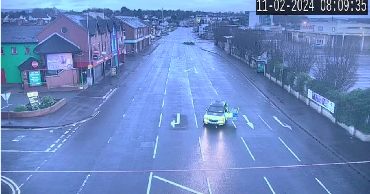 Strand Road Derry crash RECAP as one man in 'critical condition' in hospital after 'serious' crashThe road has now reopened
続きを読む »
 Driver critical after crashing into two cars in AirdriePolice say the man is being treated for 'life-threatening injuries' after he was involved in two collisions in Airdrie.
続きを読む »
 Peripheral immune factors may impact CNS function and behavior under stressResearchers report a study on the effects of psychosocial stress on the immune system and its potential impact on central nervous system (CNS) function and behavior. The study aims to advance the understanding of major depressive disorder (MDD) and develop prevention and treatment strategies.
続きを読む »
 Six surprising tales from the GP’s surgeryExamining the stress, excitement and challenges facing a 21st-century medic.
続きを読む »
 Inside King Charles’ cancer care plan as royal expert explains why he couldn’t see Harry for longer than 30...Real reason why Harry was only given 45 mins with Charles may be because of Camilla
続きを読む »
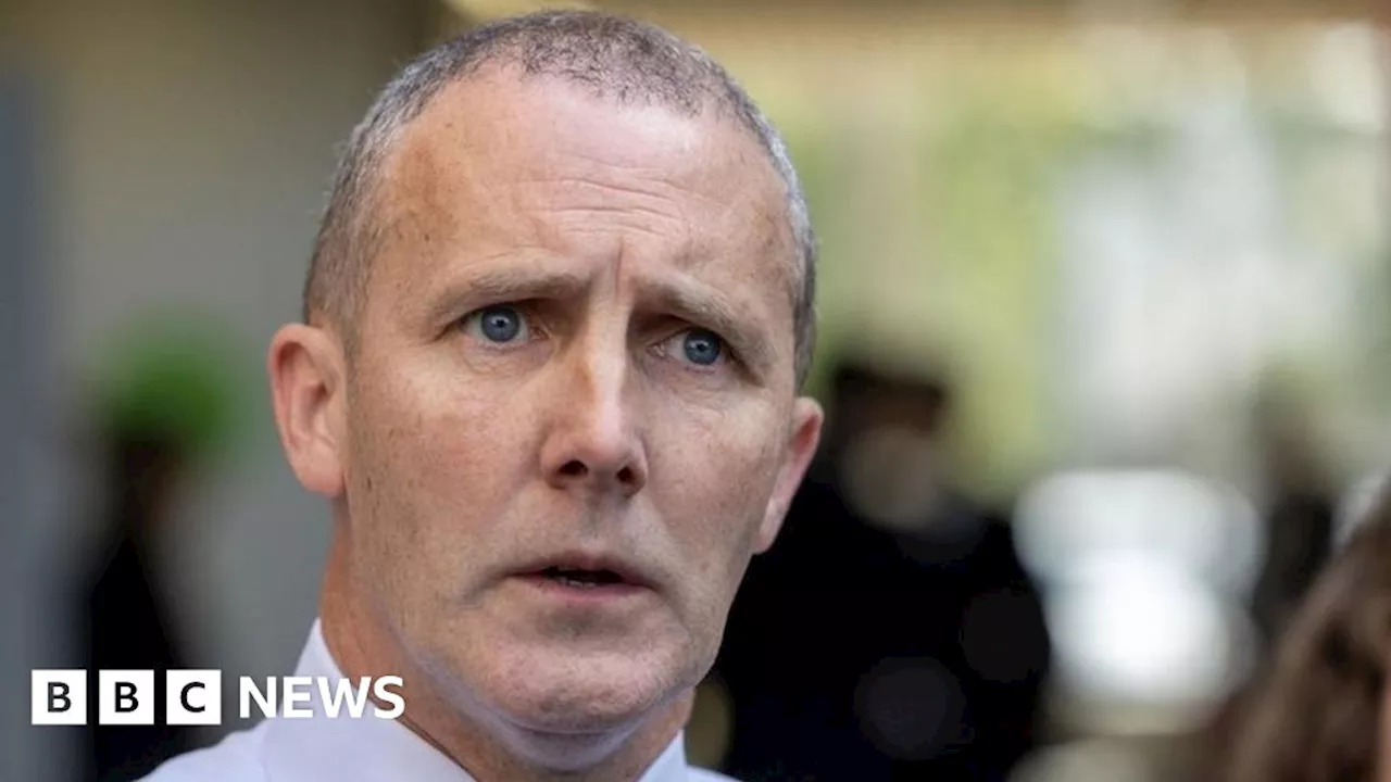 Why did iPad row minister Michael Matheson choose to quit now?The reasons why Michael Matheson resigned as health secretary on Thursday are still not entirely clear.
続きを読む »