A study showing how electrons flow around sharp bends, such as those found in integrated circuits, has the potential to improve how these circuits, commonly used in electronic and optoelectronic devices, are designed.
is titled"Mapping the intrinsic photocurrent streamlines through micromagnetic heterostructure devices" and appears in theGabor explained that when electrons gain kinetic energy they heat up. Ultimately, they heat the material around them, such as wires that can risk melting.
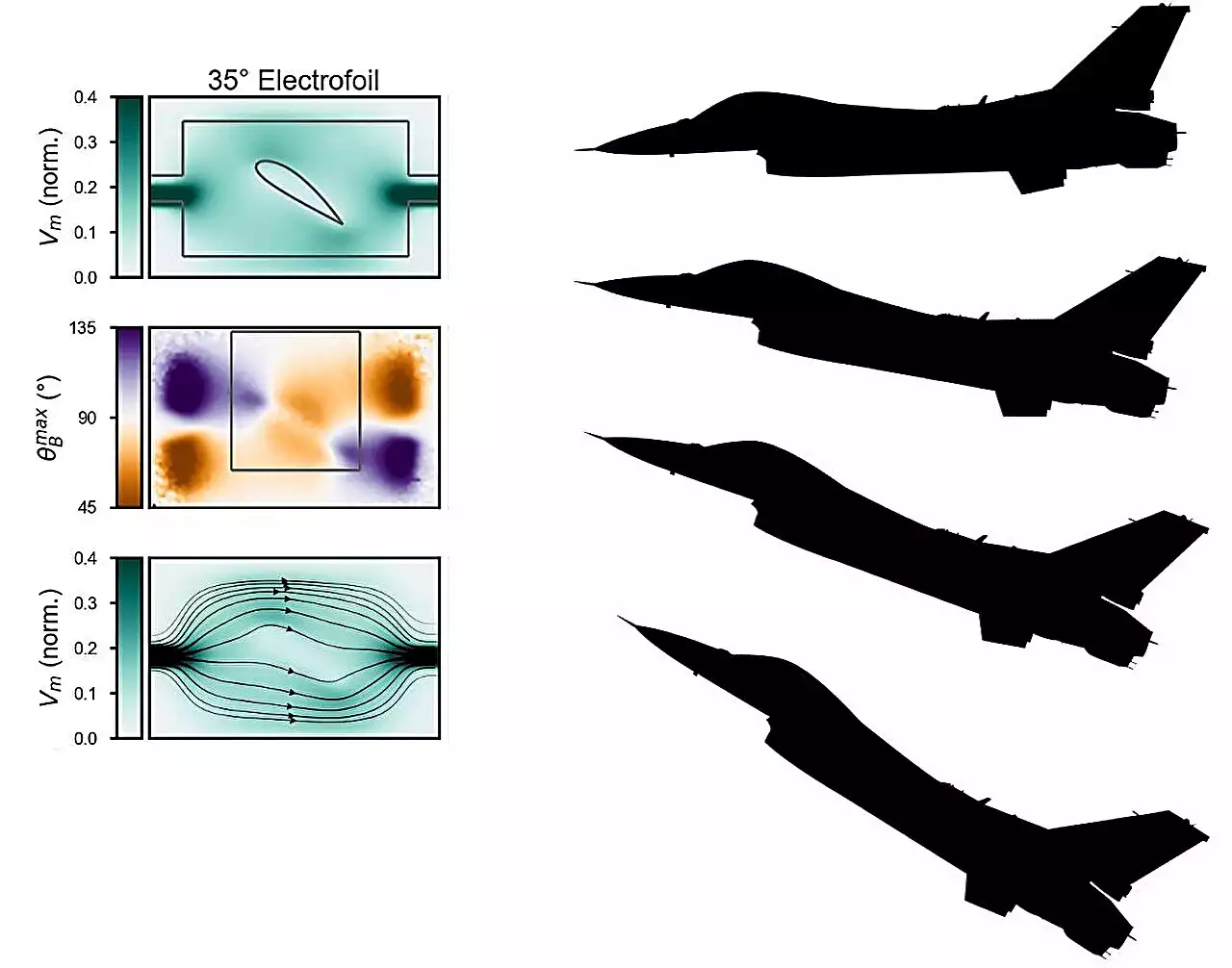
Gabor's team designed the electrofoils in the lab as little wing shapes in nanoscale devices that make the electrons flow around them, similar to how air molecules flow around an airplane wing. , we can adopt an approach with plumbing in mind and design pipelines for electrons to flow through."